THz Spectroscopy and Its Applications
Optical spectroscopy is one of the most widely used techniques for investigating chemical composition, structural properties, and light–matter interactions in solutions, thin films, and bulk materials. Depending on the spectral range of the excitation sources, spectroscopy can be classified into X-ray spectroscopy, optical spectroscopy (particularly in the visible range), electron spectroscopy, and others. X-ray spectroscopy is extensively employed to probe atomic local structures, elemental and chemical compositions, and electronic states in a wide variety of materials. In contrast, electron spectroscopy analyzes the energies of emitted or scattered electrons, enabling the identification of elements and the determination of their electronic structures. Meanwhile, bonding mechanisms and vibrational modes in molecules and solids can be explored using spectroscopic techniques based on infrared (IR) light sources, as most molecules exhibit characteristic absorption features, so-called molecular fingerprints, in the IR region of the electromagnetic spectrum (4000–400 cm–1). Here, these fingerprints correspond to resonance frequencies of specific electronic, vibrational, or spin states. However, information in the low-frequency regime below the IR range is inaccessible to conventional IR spectroscopy; instead, Raman scattering spectroscopy is typically employed to probe low-energy vibrational modes. More recently, a new spectroscopic technique has emerged that operates in the terahertz (THz) frequency regime, offering unique opportunities for material characterization. As shown in Figure 1, typical optical light sources operate at frequencies on the order of 1015 Hz, whereas THz waves are electromagnetic (EM) waves with frequencies ranging from a few hundred gigahertz (109 Hz) to several terahertz (1012 Hz). Notably, the range from approximately 0.1 to 10 THz (corresponding to wavelengths of 3 mm – 30 μm, or wavenumbers of 3 – 300 cm-1) is often referred to as the “THz gap,” since the generation and detection of EM waves in this frequency region have long been challenging due to the absence of efficient sources and suitable detectors using conventional electronic or optical techniques. Overcoming this limitation has driven the urgent development of new devices and techniques capable of operating in the THz regime.
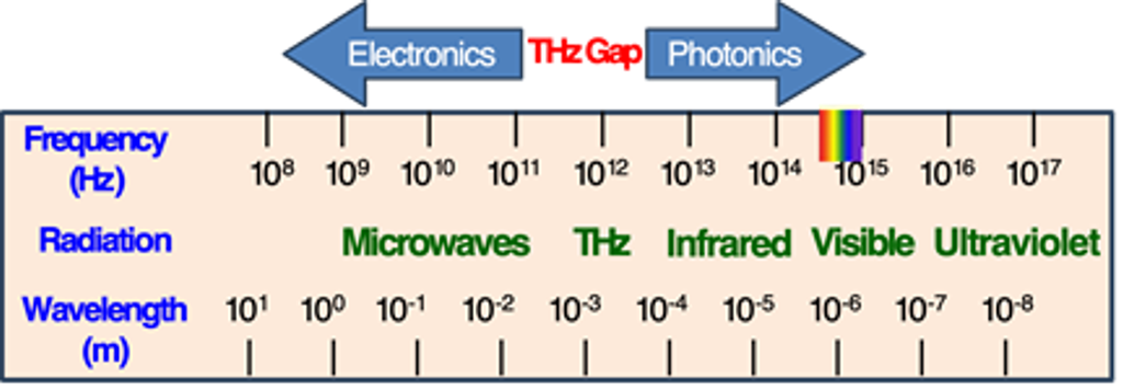 Figure 1. Spectrum of electromagnetic radiation. THz gap in the range of 0.1 to 10 THz cannot be realized by either electronic or photonic method.
With significant advances in laser technology, the generation and detection of THz waves became feasible, following the pioneering demonstration of Auston photoconductive (PC) antennas excited by ultrafast laser pulses.[1] Ultrafast lasers, with pulse durations typically on the order of sub-picoseconds (10−12 second) and high peak powers, are particularly crucial for THz generation, as they enable time-varying currents required on the picosecond timescale. Over the past decades, various THz generation techniques have been developed, including photoconductive antennas, electro-optic effects in nonlinear crystals, air or gas plasma generation, intersubband electronic transitions in quantum wells using quantum cascade lasers, and metasurface-based approaches. These techniques can produce narrowband or extremely broadband THz waves operating in either continuous-wave or pulsed modes. The photon energy of a 1 THz wave is only about 4 meV, which is several orders of magnitude lower than that of visible light or X-rays, providing THz imaging a significant advantage over many other imaging techniques. The low photon energy enables THz waves to probe electronic systems and induce transitions in a non-invasive manner, thereby minimizing sample damage or perturbation. This makes them particularly well-suited for non-destructive imaging applications, such as security screening at airports. In sharp contrast, high-energy X-rays strongly interact with matter, often inducing ionization or structural modifications in target materials.
Another distinctive advantage of THz spectroscopy lies in its detection method. In conventional optical spectroscopy, detectors typically measure only the light intensity, $I = |E|^2$, without access to the phase of the electric field. In contrast, THz detection systems directly record the time-varying electric field, $E(t)$, in the time domain using methods such as photoconductive antennas and electro-optic sampling. This direct measurement of electric field preserves both amplitude and phase information. This capability, often referred to as THz time-domain spectroscopy (THz-TDS), allows simultaneous extraction of the real and imaginary parts of optical response functions, such as refractive index, dielectric function, and optical conductivity, without resorting to Kramers–Kronig transformations. Furthermore, the sub-picosecond temporal resolution of THz-TDS allows precise probing of ultrafast carrier dynamics, and its ability to determine conductivity directly is a unique capability that conventional optical intensity detectors cannot provide.
Figure 2 shows a typical experimental setup for THz spectroscopy, employing a photoconductive (PC) antenna for THz generation and detection of THz pulses. Tightly focused femtosecond laser pulses (~100 fs) excite the emitter PC antenna at the focal point of a parabolic mirror. Because conventional glass lenses strongly absorb THz radiation, gold- or silver-coated mirrors are employed to focus and guide the THz beams. Then, the transmitted THz pulses through the sample are recorded as a function of the delay time relative to the optical probe pulse in pump-and-probe configuration. Figure 2(b) and 2(c) present a representative THz time-domain waveform and its corresponding frequency spectrum obtained by Fourier transforming the waveform in (b). In this manner, the molecular fingerprints and characteristic vibrational modes of materials can be systematically characterized in the frequency domain.
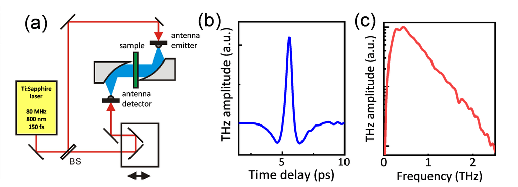 Figure 2. (a) The experimental set-up for the THz time-domain spectroscopy. A photoconductive antenna generates THz pulses under laser excitation, while a delayed probe beam enables detection using a second PC antenna. Parabolic mirrors collect and collimate the THz beam, with the sample placed in its path. (b) THz waveform obtained from time-domain measurement. (c) THz spectrum after Fourier transform of the waveform in (b).
The following section presents examples of application that leverage THz spectroscopy for probing structural vibrational modes of perovskites and characterizing the electrical properties of materials.
THz Spectroscopy for Characterization of Electrical Properties and Percolation Transition
Obtaining electrical information through an optical measurement method is particularly valuable for materials, especially nanostructures, where making electrical contacts can be challenging or may alter the intrinsic properties of the sample. Traditionally, electrical properties such as carrier concentration, mobility, and conductivity are measured using techniques like the Hall effect, which require electrodes and specific sample geometries. In contrast, THz-TDS provides a contact-free, non-destructive approach to probing these parameters, making it a powerful tool for characterizing delicate or nanoscale systems.
Highly transparent yet conductive electrode (TCE) films are essential for a wide range of optoelectronic devices, including flat-panel and plasma displays as well as solar cells. The most commonly used TCE material, indium tin oxide (ITO), offers good performance but is brittle and expensive, making it less suitable for flexible or low-cost applications. Nanostructured thin metal films, especially silver nanowire (AgNW) films, have recently emerged as promising alternatives. AgNW films can be easily deposited on almost any substrate at room temperature using simple methods such as spin coating or spray casting. They combine flexibility, transparency, and low cost, making them excellent candidates for next-generation transparent electrodes. In these films, the nanowires form a random metallic network that is highly transparent. However, as the density of nanowires increases, electrical conductivity improves at the expense of transparency, creating a tradeoff between the two properties. Therefore, achieving both high transparency and high conductivity requires carefully optimizing the nanowire density. This balance is governed by the concept of the percolation threshold, that is, when the nanowire density \( D \) is above this threshold \( D_c \), the film becomes electrically conductive, while below it, the film remains insulating.[2]
By employing THz-TDS, the complex THz conductivity of metallic AgNW films ($D \geq D_c$) was measured, as shown in Figure 3(a). The results reveal that the real part of the conductivity, $\sigma_r(\omega)$, decreases continuously with frequency, while the imaginary part, $\sigma_i(\omega)$, increases. This frequency-dependent behavior is well described by the simple Drude model.
$$\sigma(\omega) = \frac{\varepsilon_0 \, \omega_p^2 \, \tau_0}{1 - i \omega \tau_0}$$
where $\varepsilon_0$ is the absolute permittivity, $\omega_p^2 = \frac{Ne^2}{m^* \tau_0}$ is the plasma frequency, $\tau_0$ is the carrier scattering time, $N$ is the carrier density, $e$ is the electron quantity, and $m^*$ is the effective mass of carrier. Notably, the complex conductivity response of AgNW films with low NW density ($D < D_c$) exhibits a markedly different behavior from that of high-density films. As shown in Figure 3(b), $\sigma_r(\omega)$ gradually increases with frequency, while $\sigma_i(\omega)$ decreases. This unusual frequency dependence is a characteristic feature of low-dimensional materials such as nanostructures and can be effectively described by an empirical non-Drude model, namely the Drude–Smith model, expressed as [3]
$$\sigma(\omega) = \frac{\varepsilon_0 \, \omega_p^2 \, \tau_0}{1 - i \omega \tau_0} \left[ 1 + \frac{C}{1 - i \omega \tau_0} \right]$$
where $C$ is a parameter describing the fraction of the electron’s original velocity after some number of scattering events and varies between $-1$ and $0$. Then from the transitional change in the Drude–Smith parameter $C$ from $-1$ to $0$, the percolation density of AgNWs, $D_c$, can be determined, as shown in Figure 3(c). The inset depicts the schematic of an incomplete current path when $D < D_c$. In other words, the $C$ value can be used as an indicator which evaluates the connectivity between AgNWs.
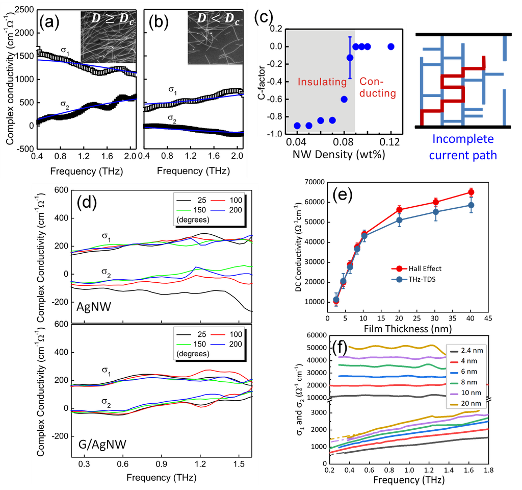 Figure 3. Complex conductivity of AgNW films as a function of frequency. The solid curves are obtained by the best fit to the data based on (a) the simple Drude and (b) the Drude-Smith model. (c) Drude–Smith C-factor as a function of NW density, showing a clear insulating-to-metallic transition. (d) THz conductivities of AgNW and graphene-covered AgNW (GAgNW) films measured at increasing annealing temperatures. (e) Comparison of conductivity measured by Hall measurement and THz-TDS. (f) Complex (real and imaginary) THz conductivity spectra of ultrathin films with thickness less than 20 nm.
THz spectroscopy also enables investigation of thermally induced percolation and stability in AgNW networks. The network retains high conductivity up to ~200 °C, far below bulk silver’s melting point (~960 °C). Above 200 °C, junction failure leads to network breakdown and performance loss in metallic network-based devices. Graphene, with high in-plane thermal conductivity, stability, and flexibility, adheres tightly to AgNW films, promoting heat dissipation and blocking gases and moisture. As shown in Figure 3(d), \( \sigma(\omega) \) of bare AgNW films exhibits a metal-to-insulator transition near 200 °C, while graphene-covered AgNW (G/AgNW) films maintain Drude-like conductivity, demonstrating enhanced thermal stability, electrical performance, and optical transparency.[4]
Besides metal nanowire networks, metal films also undergo a percolation transition as thickness increases. Noble metals such as gold (Au), when deposited by evaporation or sputtering, initially exhibit a discontinuous, rough morphology, with continuous, conductive films forming only beyond a percolation threshold of ~6–10 nm. In contrast, titanium nitride (TiN), with its rocksalt structure, can form smooth, continuous films at ultrathin thicknesses when grown by molecular beam epitaxy (MBE). The percolation thickness of TiN can also be determined using THz time-domain spectroscopy (THz-TDS).[5] Figure 3(e) shows that DC conductivities from Hall effect and THz-TDS measurements agree closely. It is in sharp contrast to ultrathin TiN films grown by other methods, where large discrepancies are typically observed between optically and electrically measured conductivities. Furthermore, Figure 3(f) reveals metallic Drude-like \( \sigma(\omega) \) behavior even at 2.4 nm, indicating a percolation thickness for MBE-grown TiN is below 2 nm. These detailed information cannot be obtained by the conventional Hall effect technique, demonstrating that THz-TDS provides complementary insights beyond those obtainable from Hall effect measurements.
Role of THz Spectroscopy in Understanding Perovskites
For decades, silicon-based solar cells have dominated the photovoltaic market owing to their high efficiency, stability, and scalability. However, despite these advantages, the fabrication of Si solar cells involves complex and costly processes, and tremendous efforts have been devoted to the search for next-generation materials with tunable properties, low-cost fabrication, and high power conversion efficiencies (PCEs). Hybrid halide perovskites are of current intense research focus owing to their great advantages of low cost, simple fabrication, strong light absorption, and good carrier mobilities. As shown in Figure 4(a), three-dimensional (3D) organic–inorganic hybrid (OIH) perovskites have a specific crystal structure (ABX3), where A is a small monovalent organic cation, B is a transition metal, and X is typically a halide ion, and can be made from a wide variety of chemical elements, giving them highly tunable optical and electronic properties. Perovskites consist of BX6 cages, with organic A cations occupying the spaces within the inorganic framework. Methylammonium lead iodide (MAPbI3) perovskite is the most widely studied, exhibiting exceptional optical and electrical properties, such as broad solar absorption and efficient charge transport, making it one of the most promising candidates for next-generation solar cells.
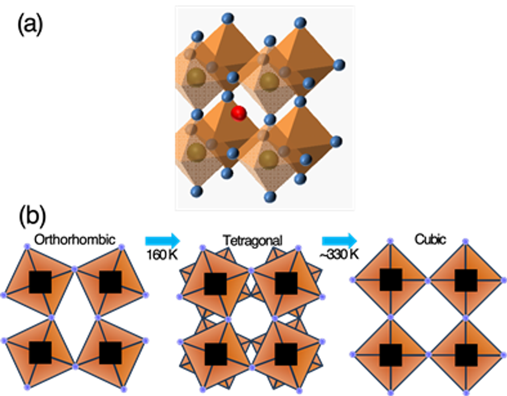 Figure 4. (a) Schematics of three-dimensional (3D) organic–inorganic hybrid perovskites. A is a small monovalent organic cation, B is a transition metal, and X is a halide ion. (b) Temperature-induced phase transition of MAPbI3 perovskite, resulting in significant changes in vibrational modes of octahedral cages.
It is well known that the symmetrical status of perovskites varies with temperature. In Figure 4(b), the room-temperature phase of MAPbI3 perovskite is tetragonal, which transforms into an orthorhombic phase below 160 K.[6] Owing to the heavy atomic mass of lead-halide components in the octahedral framework, characteristic vibrational modes, such as I–Pb–I bending and Pb–I stretching, typically appear around 1 and 2 THz, respectively. Full characterization of the different nature of stability requires a combination of several experimental techniques. Among them, the infrared/Raman spectroscopy is frequently used to realize the structural transition and vibration modes, but their sensitivity is greatly reduced in the low frequency ranges (<100 cm-1). Thus, THz-TDS with high sensitivity in the frequency range of 0.4 to 3 THz is particularly useful for characterizing the phonon modes of perovskites.
Figure 5(a) and (b) show the photoluminescence (PL) and THz conductivity spectrum for MAPbI3 perovskite as a function of temperature, respectively. Near the temperature of 160 K, the PL peak exhibits an abrupt redshift of approximately 50 nm, while the two distinct THz peaks observed at low temperatures merge into single peaks near 1 and 2 THz. These significant changes correspond to the orthorhombic-to-tetragonal phase transition of MAPbI3 perovskite. The agreement of phase transition temperature identified by PL measurement and THz spectroscopy demonstrates THz-TDS as a powerful technique for detecting structural phase transitions in perovskites.
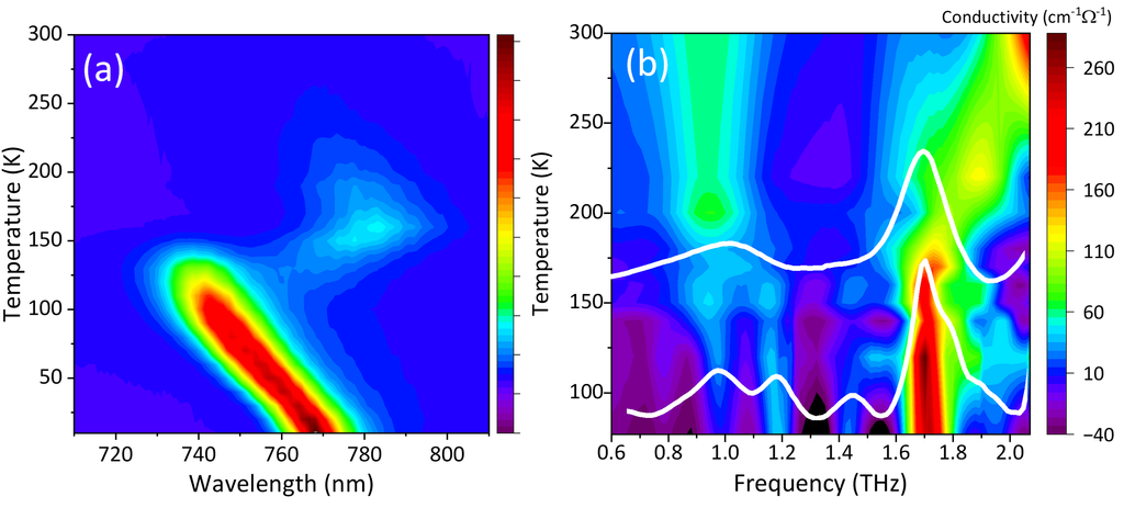 Figure 5. Contour map of temperature dependent photoluminescence (a) and THz conductivity spectrum (b) for MAPbI3 perovskite. Near the critical temperature of 160 K, the PL peak significantly redshift and the two distinct THz peaks merge into a single peak at ~1 and 2 THz. The white curves in (b) are THz conductivity measured at 50 and 170 K.
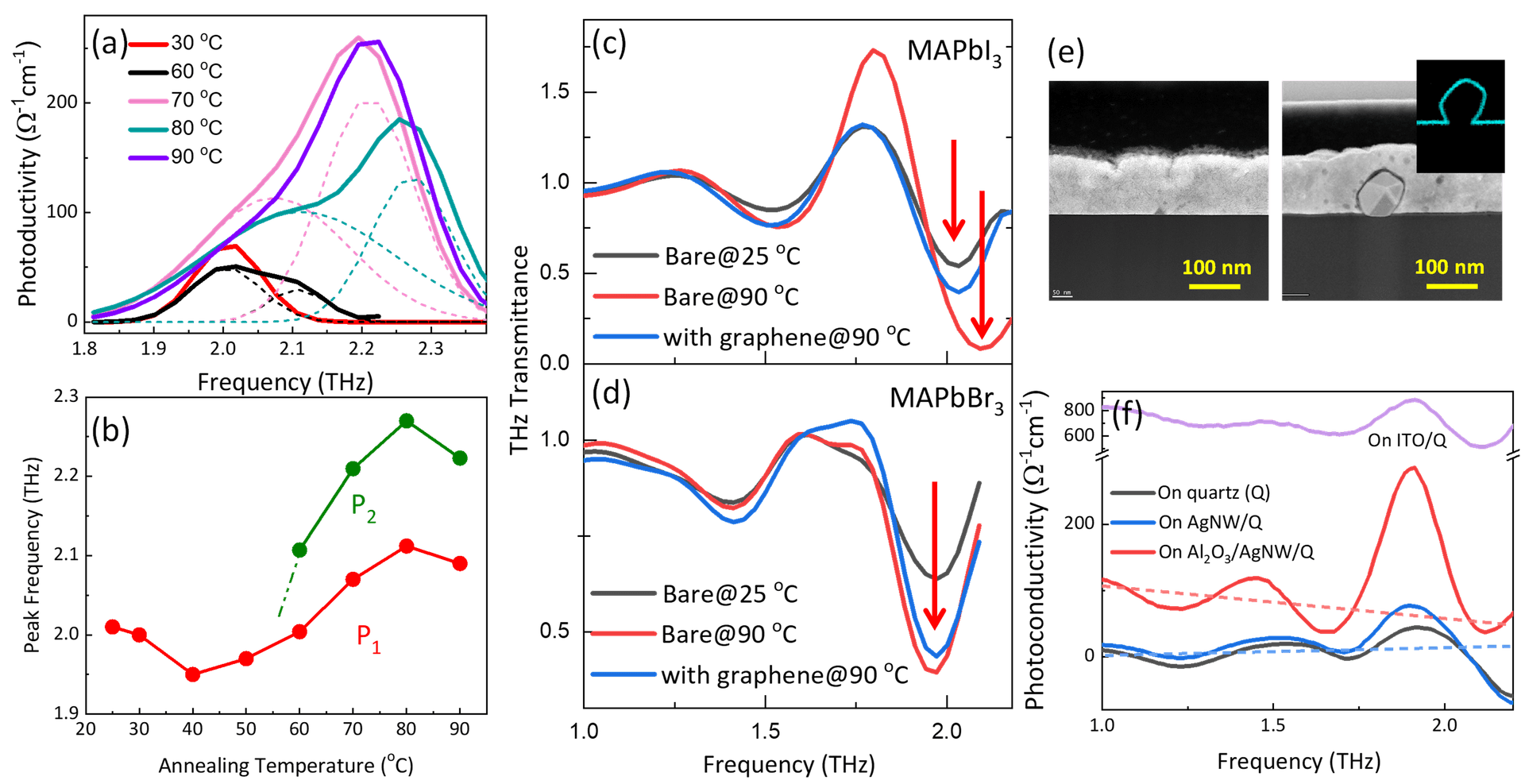
Meanwhile, the severe instabilities of MAPbI3 caused by various intrinsic and environmental factors have been raising questions about the actual device performance. Moreover, for solar cells operating outdoors under prolonged solar irradiation, continuous heating can lead to thermal instabilities. This issue is particularly critical for MAPbI₃-based solar cells, since MAPbI₃ undergoes another structural phase transition from tetragonal to cubic phase at approximately 60–65 °C, which is significantly lower than the typical maximum operating temperature of solar cells (~85 °C). Distortions in the PbI6 framework due to temperature-induced phase transition directly cause thermal instabilities in the devices. Figure 6(a) shows the THz conductivity of MAPbI₃ film as the temperature increases from room temperature to 90 °C. At temperatures below 60 ℃, there is a single peak centered at 2 THz, but at 60 ℃, a new small peak emerges at 2.1 THz.[7] In Figure 6(b), peak separation becomes more obvious and further increase in temperature results in a large peak shifting towards higher frequencies. It is similar to the mode-split of MAPbI3 at ~160 K, which is attributed to the orthorhombic-to-tetragonal phase transition.
To resolve the thermal instability at the elevated temperatures, we introduced graphene overlayer with over 100-fold anisotropy of heat flow between the in-plane and out-of-plane directions. Figure 6(c) illustrates the THz transmittance spectra for MAPbI₃. For MAPbI₃, the peak near 2 THz shifts to higher frequencies when annealed at 90 °C due to phase transition, whereas the sample with the graphene overlayer shows no such shift. To validate this observation, we performed the same measurement on another OIH perovskite, MAPbBr3, which exists in the cubic phase at room temperature. Figure 6(d) shows that despite the increase in mode strength, there is no detectable frequency shift in the THz transmittance spectrum of MAPbBr3 under annealing, confirming the efficient role of graphene overlayer for passivating heat from perovskite-based solar cells.
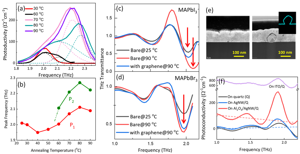 Figure 6. (a) Photoconductivity spectra and peak-fitting curves for the resonant phonon mode at ~2 THz. (b) Frequency shift of separated peaks at different annealing temperatures. (c,d) THz transmittance at 25 and 90 ℃ for MAPbI3 and MAPbBr3 with and without graphene overlayer., respectively. (e) Cross-sectional TEM images of MAPbI3/AgNW and MAPbI3 on quartz substrate, respectively. Inset shows the energy-dispersive X-ray spectroscopy mapping of the Al element. (f) Photoconductivity spectra of MAPbI3 on quartz, AgNW, and Al2O3/AgNW, along with AgNW on indium tin oxide (ITO) layer which is a conductive oxide.
Meanwhile, in the vertically integrated composite devices, a crucial instability can arise at the contact interface between different components. In particular, the TCEs in solar cells are in direct contact with the perovskite layer and their stabilities at the interface are vital in determination of the device performance. In the previous section, we demonstrated AgNW networks as excellent TCE material. However, for the MAPbI$_3$ on top of AgNW network layer (MAPbI$_3$/AgNW), the chemical reaction between Ag atoms and iodide ions causes not only a serious degradation of the perovskite layer, but also reduction of electrical conductivity of the system. Recent intense efforts found that the insertion of thin metal oxide (for example, Al$_2$O$_3$) layer can be effective in preventing the ion diffusion and chemical reaction between adjacent layers. Figure 6(e) displays the transmission electron microscopy (TEM) images of MAPbI$_3$/AgNW, in which no AgNW is found in TEM images covering the area of at least $10\ \mu\mathrm{m}$, which is much larger than the average space ($\leq 5\ \mu\mathrm{m}$) between NWs. This may be attributed to the decomposition of the unprotected AgNWs. In contrast, for MAPbI$_3$/Al$_2$O$_3$/AgNW, a pentagonal AgNW covered by the perovskite layer can be clearly observed. Furthermore, the inset presents the energy-dispersive X-ray spectroscopy mapping of the Al element, which is distributed exclusively along the contour of the AgNW, confirming that the ultrathin Al$_2$O$_3$ interlayer conformally covers the surface of AgNWs. Next, we measured $\sigma_1(\omega)$ of MAPbI$_3$ incorporated with the AgNW bottom electrode using THz-TDS method. Interestingly, Figure 6(f) shows that when the unprotected AgNWs are incorporated with MAPbI$_3$, the THz response of MAPbI$_3$/AgNW is nearly the same as that of MAPbI$_3$ single layer on quartz substrate, indicating the vanishing of the continuous conducting paths in the AgNW network after deposition of MAPbI$_3$ layer. The observed similar responses between MAPbI$_3$/quartz and MAPbI$_3$/AgNW indicate that during the solution process, the perovskite may infiltrate into the gaps of AgNWs and react with Ag atoms, causing the disconnection of percolation path in AgNW networks. Meanwhile, for MAPbI$_3$/Al$_2$O$_3$/AgNW, $\sigma_1(\omega)$ illustrates a clear Drude-like dependence on frequency with much higher DC conductivity than that of MAPbI$_3$/AgNW.
Terahertz spectroscopy has emerged as a powerful tool for probing the fundamental properties of materials. By providing direct access to low-energy excitations and phonon modes in the so-called THz gap frequency range, it reveals insights often inaccessible through conventional electrical or optical techniques. In this article, I have demonstrated through several example studies that THz spectroscopy with its high sensitivity to conductivity, vibrational fingerprints, and structural phase transitions is particularly valuable for investigating emerging materials such as perovskites, nanostructures, and ultrathin metallic films. In addition, terahertz time-domain spectroscopy enables non-contact, non-destructive, and spectrally resolved measurements of electrical properties, complementing conventional methods such as the Hall effect. Altogether, these capabilities establish THz spectroscopy not only as a fundamental research tool for understanding material properties but also as a promising technique for guiding the design and optimization of next-generation optoelectronic and energy devices.
[1]D. H. Auston, K. P. Cheung, and P. R. Smith, Picosecond photoconducting Hertzian dipoles, Appl. Phys. Lett., 45, 284-286 (1984).
[2]Y.-J. Tsai, C.-Y. Chang, Y.-C. Lai, P.-C. Yu, and H. Ahn, Realization of metal−insulator transition and oxidation in silver nanowire percolating networks by terahertz reflection spectroscopy, ACS Appl. Mater. Interfaces 6, 630 (2014).
[3]N.V. Smith, Classical generalization of the Drude formula for the optical conductivity Phys. Rev. B, 64, 155106–4 (2001).
[4]J.-Z. Chen, H. Ahn, S.-C. Yen, and Y.-J. Tsai, “Thermally induced percolational transition and thermal stability of silver nanowire networks studied by THz spectroscopy,” ACS Appl. Mater. Interfaces, 6, 20994 (2014).
[5]I Hong Ho, C.-W. Chang, Y.-L. Chen, W.-Y. Chang, T.-J. Kuo, Y.-J. Lu, S. Gwo, and H. Ahn, Ultrathin TiN epitaxial films as transparent conductive electrodes, ACS Appl. Mater. Interfaces. 14, 16839–16845 (2022).
[6]Whitfield, P., Herron, N., Guise, W. et al. Structures, phase transitions and tricritical behavior of the hybrid perovskite methyl ammonium lead iodide. Sci Rep 6, 35685 (2016).
[7]Z.-W. Huang, Y.-H. Hong, Y.-J. Du, T.-J. Kuo, C.-C. Huang, T. S. Kao, and H. Ahn, THz analysis of CH3NH3PbI3 perovskites associated with graphene and silver nanowire electrodes, ACS Appl. Mater. Interfaces. 13, 9224–9231 (2021).

